









BLOG
Top 10 Fatal EMI and Compliance Mistakes OEMs Make When Switching to GaN
QUICK LINKS
Why EMI Becomes a Critical Failure Point When OEMs Transition to GaN
GaN technology introduces a fundamental shift in power electronics design. While it enables higher efficiency, smaller form factors, and improved power density, it also introduces one of the most dangerous hidden risks in modern adapter design: uncontrolled electromagnetic interference. The same high-speed switching behavior that makes GaN so attractive also makes it far more prone to generating high-frequency noise, which can propagate through PCB traces, cables, and enclosures in unpredictable ways.
For OEMs, this is not just a technical challenge. It is a business risk. A product that fails electromagnetic compatibility testing can be blocked from market entry entirely. Regulatory bodies such as the Federal Communications Commission (FCC) enforce strict limits on unintentional radiators under Part 15 (https://www.fcc.gov/oet/ea/rules/part15), and failing these requirements can delay product launches by months. In many cases, it forces full PCB redesigns, additional shielding, and repeated testing cycles that significantly increase development costs.
This is why EMI must be treated as a core design discipline from the beginning. It is not something that can be fixed at the end of the process. Phihong’s GaN platform strategy reflects this reality by integrating EMI mitigation directly into design architecture, rather than treating it as a secondary consideration.
Useful Links
- https://www.phihong.com/best-guide-to-gan-power-supplies-for-oems-industrial-medical-telecom/
- https://www.phihong.com/products/adapters/
- https://www.phihong.com/how-gallium-nitride-gan-is-powering-the-next-generation-of-compact-high-efficiency-robot-power-supplies/
Related Articles
- https://www.phihong.com/top-10-features-oems-should-look-for-in-a-high-density-gan-power-adapter/
- https://www.phihong.com/top-10-gan-power-supply-trends-oems-need-to-know-in-2026-and-beyond/
- https://www.phihong.com/top-10-ways-gan-is-changing-thermal-design-in-compact-high-power-adapters/
FEATURED PRODUCTS
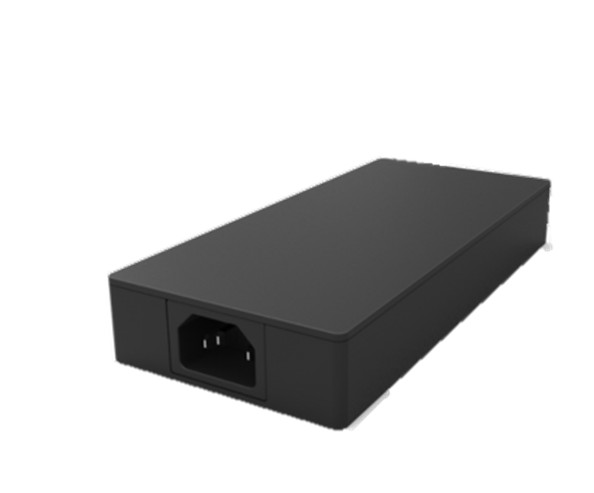
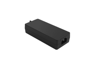
AA240U-200A-R
- Output Power - 240W
- Output Volt - 20V
- Output Current - 12A
- Features - high-efficiency desktop power supply designed for multiple applications, delivering a reliable 240W single output with advanced GaN technology for compact performance. Ideal for powering high-demand gaming systems etc with reduced heat and improved energy conversion.
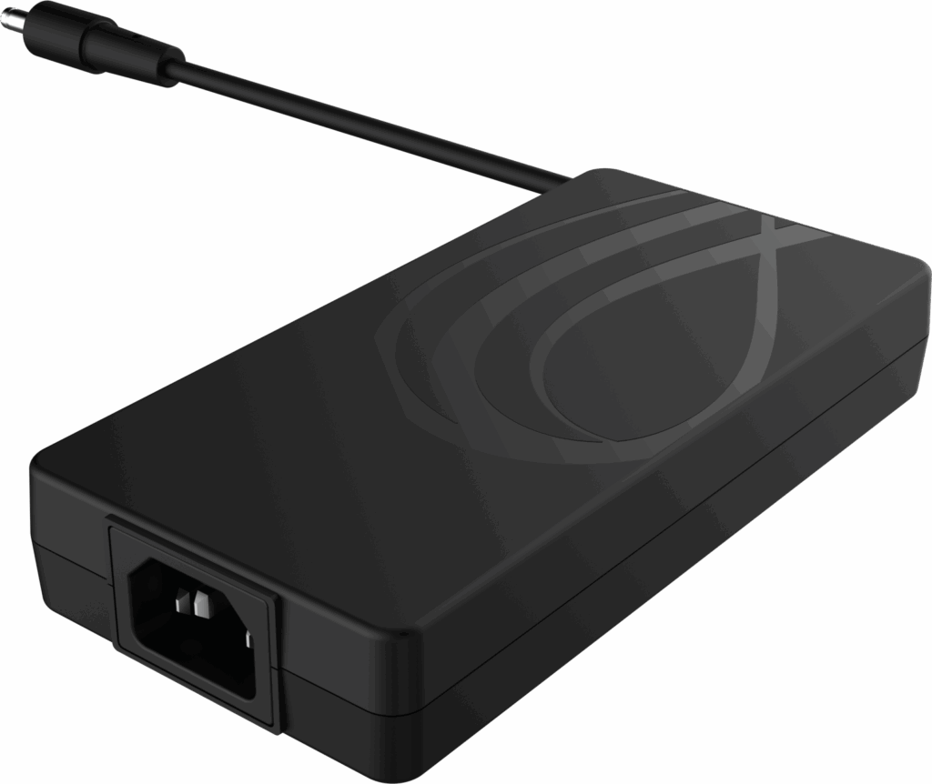
AA240U-200B-R
- Output Power - 240W
- Output Volt - 20V
- Output Current - 12A
- Features - This 240-watt GaN Series Desktop C14 Adapter delivers high power in a compact, efficient design, ideal for demanding professional and industrial applications. Its GaN technology ensures cooler operation, reliability, and space-saving performance.
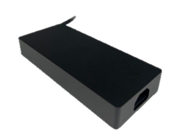
AA280U-200B-R
- Output Power - 280W
- Output Volt - 20V
- Output Current - 14A
- Features - high-efficiency desktop power supply designed for multiple applications, delivering a reliable 240W single output with advanced GaN technology for compact performance. Ideal for powering high-demand gaming systems etc with reduced heat and improved energy conversion.
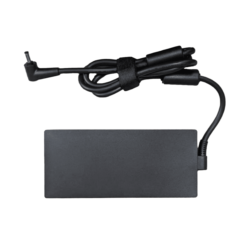
AM330U-200B(A)-R
- Output Power - 330W
- Output Volt - 20V
- Output Current - 16.5A
- Features - GaN (Gallium Nitride) Technology, DoE Level VI Compliance, 5,000 Meters Operating Altitude, Peak Load Capability, & 1” Low Profile Splash-Proof Case with IEC 60320 C14 Inlet

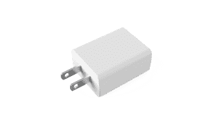
AQ18A-59CFC-H
- Output Power - 18W
- Output Volt - 5V/9V/12V/15V
- Output Current - 3A/2A/1.5A/1.2A
- Features - USB-C PD 3.0 Certified, Small Form Factor/High Power Density, DOE VII , Class B EMI, utilizes GAN technology to have an improved efficiency and faster charging while decreasing the size and weight of the product
- Application: Mobile Phone • Networking Devices • Tablet • Monitor etc

AQ18E-59CFC-H
- Output Power - 18W
- Output Volt - 5V/9V/12V/15V
- Output Current - 3A/2A/1.5A/1.2A
- # of ports - 1
- Features - USB-C PD 3.0 Certified, Small Form Factor/High Power Density, DOE VII , Class B EMI, COC Version 5 Tier 6, utilizes GAN technology to have an improved efficiency and faster charging while decreasing the size and weight of the product
- Application: Mobile Phone • Networking Devices • Tablet • Monitor

AQ18K-59CFC-H
- Output Power - 18W
- Output Volt - 5V/9V/12V/15V
- Output Current - 3A/2A/1.5A/1.2A
- # of ports - 1
- Features - USB-C PD 3.0 Certified, Small Form Factor/High Power Density, DOE VII , Class B EMI, COC Version 5 Tier 7,utilizes GAN technology to have an improved efficiency and faster charging while decreasing the size and weight of the product
- Application: Mobile Phone • Networking Devices • Tablet • Monitor etc
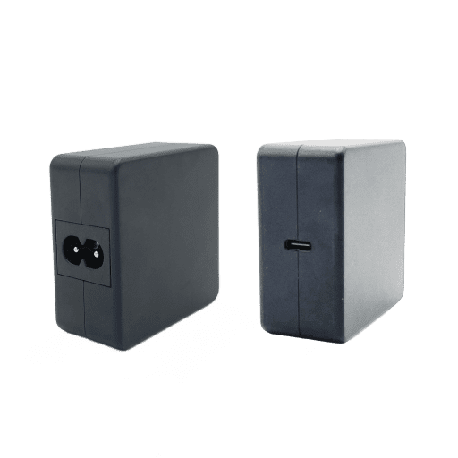
AQ60W-59FKKA-R
- Output Power - 60W
- Output Volt - 5V/9V/15V/20V
- Output Current - 3A/3A/3A/3A
- # of ports - 1
- Features - GaN Technology, USB Power Delivery 3.0, DoE Level VI Compliance, CoC Version 5 Tier 2 Compliance, 5,000 Meters Operating Altitude, Suitable for commercial and consumer electronic products

AQ65A-59FKB-R
- Output Power - 65W
- Output Volt - 5V/9V/15V/20V (PPS : 3.3V~21V)
- Output Current - 3A/3A/3A/3A
- # of ports - 1
- Features - GaN Technology, USB Power Delivery 3.0, DoE Level VI Compliance, CoC Version 5 Tier 2 Compliance, 5,000 Meters Operating Altitude, Suitable for commercial and consumer electronic products

AQ65E-59FKB-R
- Output Power - 65W
- Output Volt - 5V/9V/15V/20V (PPS : 3.3V~21V)
- Output Current - 3A/3A/3A/3A
- # of ports - 1
- Features - GaN Technology, USB Power Delivery 3.0, DoE Level VI Compliance, CoC Version 5 Tier 2 Compliance, 5,000 Meters Operating Altitude, Suitable for commercial and consumer electronic products

AQ65F-59FKA-R
- Output Power - 65W
- Output Volt - 5V/9V/15V/20V
- Output Current - 3A/3A/3A/3.25A
- # of ports - 1
- Features - GaN Technology, USB Type-C Foldable DoE Level VI Compliance, 5,000 Meters Operating Altitude, Suitable for commercial and consumer electronic products

AQ65K-59FKB-R
- Output Power - 65W
- Output Volt - 5V/9V/15V/20V (PPS : 3.3V~21V)
- Output Current - 3A/3A/3A/3A
- # of ports - 1
- Features - GaN Technology, USB Power Delivery 3.0, DoE Level VI Compliance, CoC Version 5 Tier 2 Compliance, 5,000 Meters Operating Altitude, Suitable for commercial and consumer electronic products

Why Traditional EMI Design Rules Break Down with GaN Architectures
Traditional silicon-based power designs operate at lower switching frequencies, which naturally limits the amount of high-frequency noise generated. Engineers have spent decades refining layout techniques and filtering methods around these constraints. However, GaN devices operate at much faster switching speeds with sharper voltage transitions, creating a completely different electromagnetic environment.
These fast transitions generate higher dv/dt and di/dt values, which significantly increase radiated and conducted emissions. Even small layout inefficiencies can act as antennas, amplifying noise across the system. This is why many GaN designs that appear stable during initial testing fail compliance in final certification labs.
Engineering research available through IEEE Xplore (https://ieeexplore.ieee.org) consistently highlights the need for advanced EMI mitigation strategies in high-frequency switching systems. These include tighter PCB layouts, optimized grounding, and improved shielding techniques. Similarly, organizations like the Power Sources Manufacturers Association (https://www.psma.com) emphasize that EMI must be considered a system-level issue rather than an isolated component problem.
For OEMs, this means abandoning the idea of “copying” silicon designs and instead adopting GaN-specific design methodologies. Without this shift, even well-designed products can become noisy liabilities.
Useful Links
- https://www.phihong.com/how-to-design-internal-medical-power-systems-isolation-emc-and-compliance-explained/
- https://www.phihong.com/how-to-choose-the-best-power-adapter-supplier-for-oems-key-factors-for-safety-reliability-and-compliance/
- https://www.phihong.com/usb-c-charger-shaping-the-future-of-the-tech-world/
Related Articles
- https://www.phihong.com/medical-power-supply-how-to-choose-the-best-solution-for-safe-reliable-medical-devices/
- https://www.phihong.com/medical-power-supply-vs-medical-power-adapter-whats-the-difference-and-which-one-do-you-need/
- https://www.phihong.com/best-guide-to-medical-power-supplies-for-modern-medical-devices/
CLIENT'S QUOTE
Phihong’s custom OEM power solutions have transformed our product development, boosting performance and reducing overhead. Their expert engineering support has simplified both the design and manufacturing phases.
Top 10 Fatal EMI and Compliance Mistakes OEMs Make When Switching to GaN
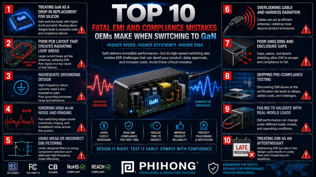
1. Treating GaN as a Drop-In Replacement for Silicon
One of the most dangerous assumptions OEMs make is that GaN can simply replace silicon without requiring design changes. While the electrical function may appear similar, the switching behavior is dramatically different. GaN devices switch much faster, which increases high-frequency noise and electromagnetic emissions.
When engineers reuse silicon-based layouts, they often unknowingly introduce large loop areas, poor grounding paths, and inadequate filtering. These issues may not be visible in early testing but become critical during compliance evaluation. As outlined in FCC Part 15 guidelines (https://www.fcc.gov/oet/ea/rules/part15), even small increases in radiated emissions can push a product beyond acceptable limits.
To avoid this, OEMs must redesign their power architecture with GaN in mind. This includes optimizing PCB layout, reducing loop areas, and implementing proper shielding strategies. Treating GaN as a fundamentally different technology is the first step toward avoiding costly EMI failures.
2. Poor PCB Layout That Creates Radiating Loop Areas
PCB layout is one of the most critical factors in EMI performance. In high-frequency GaN designs, current loops can act as antennas, radiating noise across the system. Large loop areas increase electromagnetic emissions and make it difficult to pass compliance testing.
Engineers must minimize loop areas by placing components strategically and routing traces efficiently. This includes keeping high-current paths short and tightly coupled. Research from IEEE (https://www.ieee.org) consistently emphasizes the importance of loop control in high-frequency power systems.
Failure to optimize PCB layout often leads to excessive radiated emissions, requiring additional shielding or redesign. This is one of the most common causes of certification delays in GaN-based products.
3. Inadequate Grounding and Poor Return Path Design
Grounding is often misunderstood in power electronics design. In GaN systems, improper grounding can create unintended noise paths that interfere with sensitive circuits. Poor return paths increase impedance and allow noise to propagate throughout the system.
Engineers must design low-impedance ground paths and ensure that return currents follow controlled routes. This reduces noise coupling and improves overall system stability. Organizations like PSMA (https://www.psma.com) highlight grounding as a key factor in EMI mitigation.
Without proper grounding, even well-designed circuits can exhibit unpredictable behavior. This makes it difficult to achieve consistent performance across different operating conditions.
4. Ignoring High dv/dt Effects in GaN Switching
GaN devices generate extremely fast voltage transitions, resulting in high dv/dt. These rapid changes can cause capacitive coupling between components, leading to unwanted noise and interference.
If not managed properly, high dv/dt can disrupt nearby circuits, including sensors and communication modules. This is particularly problematic in compact designs where components are closely spaced.
Engineers must consider dv/dt effects when selecting components and designing layouts. This includes using proper spacing, shielding, and filtering techniques to minimize noise propagation.
5. Underestimating the Need for Advanced EMI Filtering
Filtering is essential for controlling conducted emissions, but many designs rely on filters optimized for silicon-based systems. These filters may not be effective for GaN’s higher switching frequencies.
Proper EMI filter design requires balancing noise suppression with efficiency and leakage current. This is especially important in medical and industrial applications where safety standards are strict.
Phihong’s GaN designs incorporate optimized filtering to address these challenges. OEMs must ensure that their filtering strategy is tailored to GaN’s unique characteristics to avoid compliance issues.
6. Overlooking Cable Radiation and Connector EMI Leakage
One of the most underestimated EMI sources in GaN designs is not the PCB itself, but the cable and connector system. High-frequency switching noise can travel along output cables and radiate into the surrounding environment, effectively turning the power cord into an unintended antenna.
This issue becomes more pronounced in compact high-power adapters, where higher switching frequencies create stronger high-frequency harmonics. Without proper shielding, ferrite components, and cable routing strategies, emissions can easily exceed regulatory limits.
According to FCC Part 15 requirements (https://www.fcc.gov/oet/ea/rules/part15), radiated emissions must remain within strict thresholds, regardless of whether the noise originates internally or through external cables. Engineers must therefore treat cables as part of the EMI system, not as passive accessories.
OEMs should implement shielded cables, optimized connector grounding, and proper filtering at the output stage. Ignoring this area often leads to unexpected test failures late in development.
7. Weak Shielding and Poor Enclosure Design
Shielding is one of the most effective ways to control EMI, but it is often applied too late in the design process. In GaN-based systems, where noise levels are higher, weak or incomplete shielding can allow emissions to escape and interfere with nearby devices.
Enclosure design plays a critical role in this. Gaps, seams, and poorly grounded metal surfaces can reduce shielding effectiveness and create leakage paths for electromagnetic noise. This is especially problematic in compact adapters where space constraints limit shielding options.
Engineering best practices from organizations like the Power Sources Manufacturers Association (https://www.psma.com) emphasize that shielding must be integrated into the design from the beginning. It should not be treated as a last-minute fix.
For OEMs, investing in proper enclosure design early can prevent costly redesigns and ensure smoother compliance testing.
8. Skipping Pre-Compliance Testing and Iterative Validation
Many OEMs rely solely on final certification testing to validate EMI performance. This is a major risk. If a design fails at this stage, the cost and time required to fix the issue can be substantial.
Pre-compliance testing allows engineers to identify and resolve EMI problems early in the development cycle. This includes using spectrum analyzers, near-field probes, and test chambers to evaluate emissions under different conditions.
Engineering guidelines from IEEE (https://www.ieee.org) highlight the importance of iterative testing in high-frequency power systems. By validating designs throughout development, engineers can avoid surprises during final certification.
OEMs that skip this step often face delays, increased costs, and missed market opportunities.
9. Failing to Validate EMI Performance Under Real Load Conditions
EMI behavior can vary significantly depending on load conditions. A power supply that performs well at nominal load may exhibit different characteristics under peak or dynamic loads.
GaN adapters, with their fast switching speeds, are particularly sensitive to these variations. Changes in load can alter switching behavior, affecting both conducted and radiated emissions.
OEMs must test their designs across a full range of operating conditions, including maximum load, transient spikes, and idle states. This ensures consistent performance and reduces the risk of unexpected failures.
Ignoring this step can lead to products that pass initial tests but fail under real-world usage.
10. Treating EMI as a Final Step Instead of a Core Design Principle
The most critical mistake OEMs make is treating EMI as something to address at the end of development. In GaN designs, this approach does not work.
EMI must be considered from the very beginning of the design process. This includes PCB layout, grounding, component selection, and enclosure design. Waiting until the end to address EMI often results in major redesigns.
Standards organizations like IEC (https://www.iec.ch) and regulatory bodies such as the FCC emphasize that compliance is not just about testing. It is about designing systems that inherently meet emission requirements.
For OEMs, adopting a proactive approach to EMI design is essential. It reduces risk, improves product quality, and accelerates time to market.
Why EMI Mistakes Are So Costly for OEMs
EMI failures are not just technical issues. They are business risks that can impact product timelines, budgets, and reputation.
A failed compliance test can delay a product launch by months, requiring redesign, re-testing, and additional certification costs. In competitive markets, this delay can result in lost revenue and missed opportunities.
More importantly, EMI issues can affect product performance. Noise interference can disrupt sensors, displays, and communication systems, leading to unreliable operation. For medical and industrial devices, this can have serious consequences.
By understanding and avoiding these common mistakes, OEMs can build more robust and reliable products. This requires treating EMI as a core design discipline and investing in proper engineering practices from the start.
Useful Links
- https://www.phihong.com/products/adapters/
- https://www.phihong.com/best-guide-to-gan-power-supplies-for-oems-industrial-medical-telecom/
- https://www.phihong.com/how-to-choose-the-best-power-adapter-supplier-for-oems-key-factors-for-safety-reliability-and-compliance/
Related Articles
- https://www.phihong.com/top-10-features-oems-should-look-for-in-a-high-density-gan-power-adapter/
- https://www.phihong.com/top-10-gan-power-supply-trends-oems-need-to-know-in-2026-and-beyond/
- https://www.phihong.com/top-10-ways-gan-is-changing-thermal-design-in-compact-high-power-adapters/
How Phihong Helps OEMs Avoid EMI and Compliance Pitfalls
Phihong’s GaN platforms are designed with EMI control as a core requirement. By integrating optimized layouts, advanced filtering, and effective shielding, Phihong helps OEMs achieve compliance more efficiently.
This approach reduces the risk of certification failure and shortens development timelines. It also improves overall product reliability by ensuring stable performance in real-world environments.
Phihong’s expertise in power supply design allows OEMs to focus on their core products while relying on proven power solutions that meet both performance and compliance requirements.
As GaN adoption continues to grow, OEMs that prioritize EMI design will be better positioned to succeed in competitive markets.

CONTACT US TODAY
From concept to production, Phihong delivers custom OEM power solutions tailored to your specifications.
POE technology supports the centralization of power

AC Adapter Guide: Everything You Need to Know
Moreover, PoE technology supports the centralization of power management. By powering devices through a PoE-enabled network …
AC DC Power Chargers and How They Work: A Comprehensive Technical Breakdown
Moreover, PoE technology supports the centralization of power management. By powering devices through a PoE-enabled network …

USB-C Charger: Shaping the Future of the Tech World
Moreover, PoE technology supports the centralization of power management. By powering devices through a PoE-enabled network …

AC Adapter Guide: Everything You Need to Know
Moreover, PoE technology supports the centralization of power management. By powering devices through a PoE-enabled network …

AC DC Power Chargers and How They Work: A Comprehensive Technical Breakdown
Moreover, PoE technology supports the centralization of power management. By powering devices through a PoE-enabled network …

USB-C Charger: Shaping the Future of the Tech World
Moreover, PoE technology supports the centralization of power management. By powering devices through a PoE-enabled network …